Keynotes
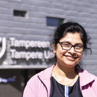
Sayani Majumdar, Tampere, University, Finland
Bio: Dr. Sayani Majumdar is an Associate Professor of Electrical Engineering at the Faculty of Information Technologies and Communication Sciences at Tampere University, Finland. She is also a visiting professor at the Miin Wu School of Computing at National Cheng Kung University, Taiwan. Her career in semiconductor device research spans more than two decades where she worked in both academia and in close collaboration with the industry. She worked on several emerging technologies in world-leading organizations including MIT, USA and Max-Planck Institute, Germany. Her team’s current research focuses on the development of non-volatile memories and neuromorphic computing hardware using low-thermal budget ferroelectric and semiconductor materials and processes for their back-end-of-line integration with CMOS circuits for their application in low-power neuromorphic edge devices.
Abstract: The quest for energy-efficient, scalable neuromorphic computing has elevated compute-in-memory (CIM) architectures to the forefront of hardware innovation. While memristive memories such as resistive random-access memories (RRAMs), phase-change memory (PCM), magneto resistive random-access memory (MRAM), ferroelectric random-access memories (FeRAM) have been extensively explored for synaptic implementation in CIM architectures, their inherent limitations, including static power dissipation, sneak-path currents, and interconnect voltage drops, pose significant challenges for large-scale deployment, particularly at advanced technology nodes. In contrast, capacitive memories offer a compelling alternative by enabling charge-domain computation with virtually zero static power loss, intrinsic immunity to sneak paths, and simplified selector-less crossbar operation, while offering superior compatibility with 3D Back-end-of-Line (BEOL) integration. This talk will highlight the architectural and device-level advantages of emerging non-volatile capacitive synapses, including metal–ferroelectric–metal (MFM), metal–ferroelectric–semiconductor (MFS), ferroelectric field-effect transistors (FeFETs), and hybrid configurations. I will present how material engineering and interface control can modulate synaptic behavior, capacitive memory window (CMW), and multilevel analog storage potential. Furthermore, I will explain critical system-level trade-offs involving device-to-device variation, charge transfer noise, dynamic range, and effective analog resolution bringing to the conclusion that capacitive memories, with custom-built stacks, have the potential to become a foundational technology for the next generation of extremely energy-efficient neuromorphic computing platforms.

Wladek Grabinski, IHP OpenPDK Consultant, Germany
Bio: Wladek Grabinski, PhD, is a semiconductor modeling expert with over 30 years of experience in advanced CMOS, RF BiCMOS technologies. He earned his doctorate from ITE, Warsaw, in 1991, then as a postdoc at ETHZ and EPFL contributed to process characterization and compact MOSFET model development. Formerly with Motorola/FSL in Geneva, he now consults on advanced SPICE modeling, Verilog-A standardization, and low-power analog/RF IC applications within IHP OpenPDK Initiative. Wladek authored the “Compact/SPICE Modeling” chapter in the Springer Handbook of Semiconductor Devices also has edited three other books and published over 70 papers. He has established the ESSERC Track3 on SPICE modeling, was also involved in TPCs of IEEE EDTM, ITRS, SBMicro, LADEC, SISPAD, MIXDES; has mentored EPFL IEEE Student Branch and now is the IEEE EDS R8 Chair. Since 1999, Wladek is managing MOS-AK workshop series to promote OpenPDK tools flow and FOSS IC design.
Abstract: The momentum behind Europe’s semiconductor sovereignty is increasingly fueled by the rise of fully open-source CAD/EDA workflows for IC design. This talk presents a comprehensive overview of the FOSS IC design flow, spanning schematic capture, simulation, verification, layout, and digital synthesis, built on interoperable tools such as Qucs-S, Xschem, ngspice, Xyce, OpenVAF, OpenEMS, Magic, kLayout, and OpenRoad. These tools establish a reproducible and extensible design ecosystem that supports both analog/RF and digital SoC developments. Recent advances in OpenPDKs from SkyWater, GF, and IHP have unlocked new opportunities for collaborative design, enabling engineers, researchers, and students across Europe to contribute to chip innovation without proprietary barriers. This open infrastructure supports Verilog-A standardization, compact modeling, and SPICE-level simulation, while also facilitating layout verification and digital place-and-route as a full open-source stack. In addition to OpenPDK IC design capabilities, the talk addresses the strategic role of open-source workflows in strengthening Europe’s semiconductor workforce, fostering reproducible research, and accelerating education and innovation across borders.